Field Effect Transistors (FET) Models


Print Profile(1)
Description
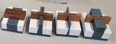
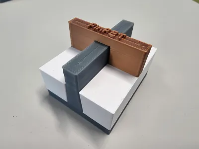
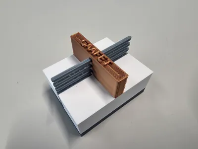
Model of various field-effect transistor semiconductor layouts: Planar FET, FINFET, GAAFET, and Nanosheet FET
Supports are a bit annoying to remove from the GAAFET and Nanosheet. I could imagine it would be easier if you rotate the models by 90 degrees and only have supports at the gate. But I haven't tried it, instead I preferred to work with a scalpel.
License
You shall not share, sub-license, sell, rent, host, transfer, or distribute in any way the digital or 3D printed versions of this object, nor any other derivative work of this object in its digital or physical format (including - but not limited to - remixes of this object, and hosting on other digital platforms). The objects may not be used without permission in any way whatsoever in which you charge money, or collect fees.
Comment & Rating (0)