
MOSFET Evolution 3D Display (Planar–FINFET-GAAFET)
Print Profile(1)

Description
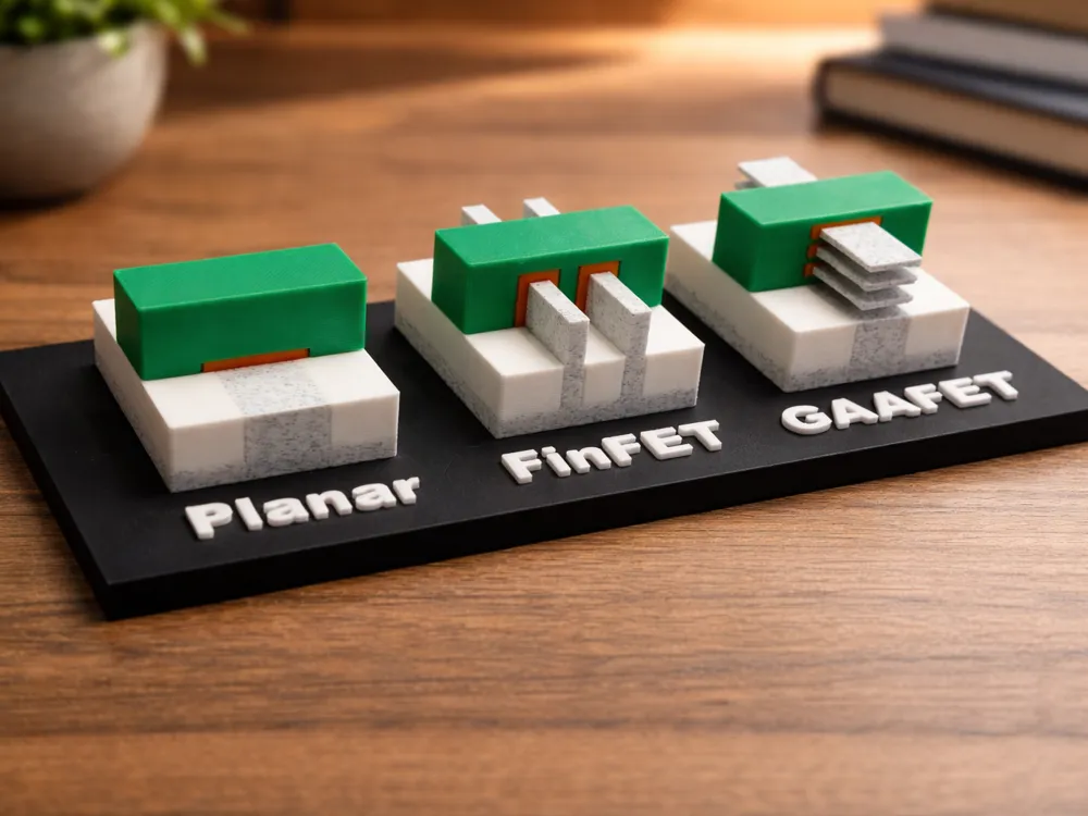
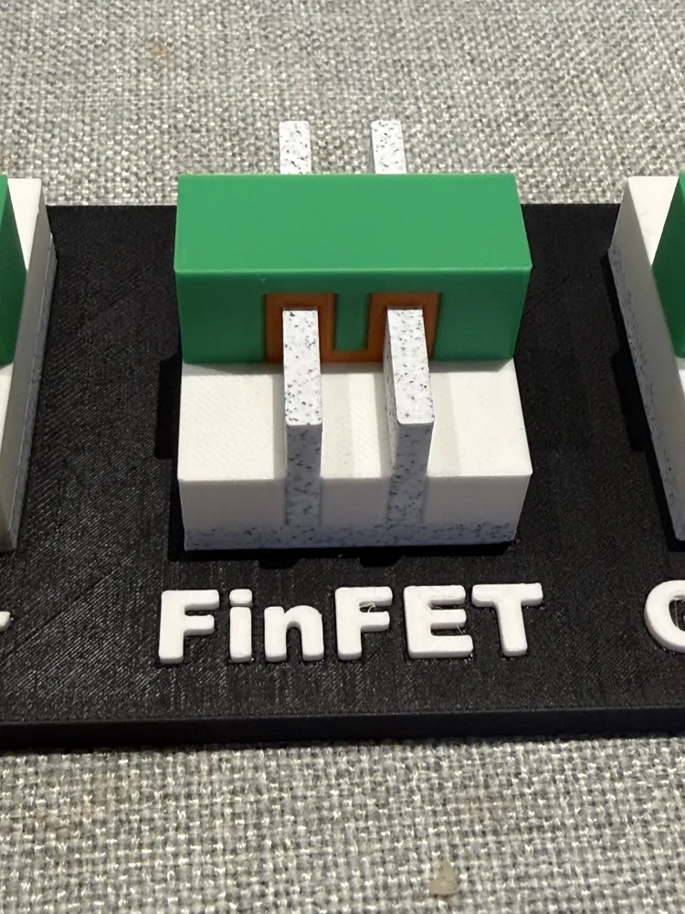
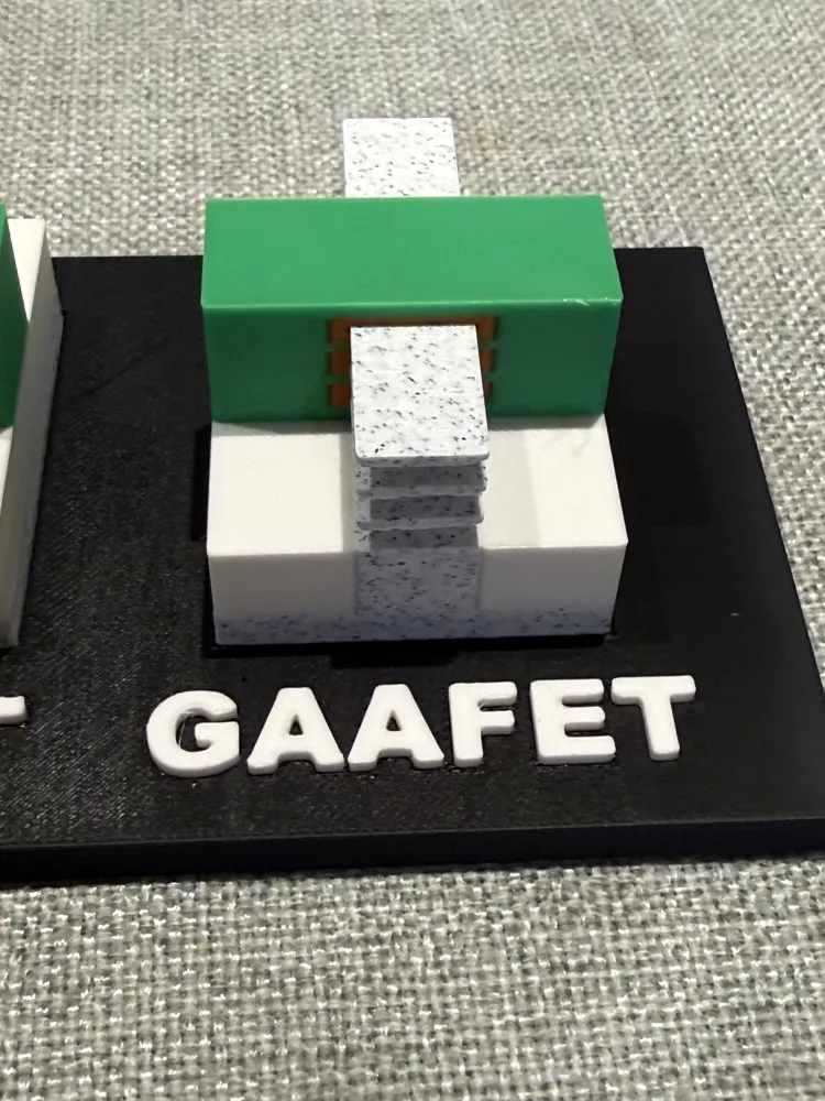
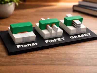
Bring semiconductor technology to life with this high-quality 3D printable MOSFET evolution display!
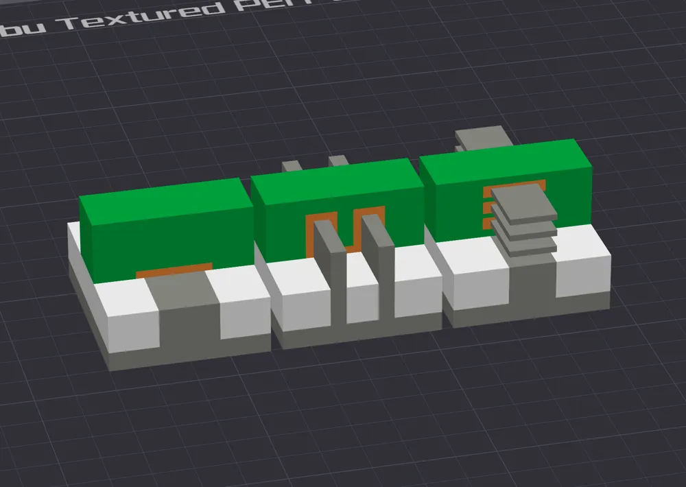
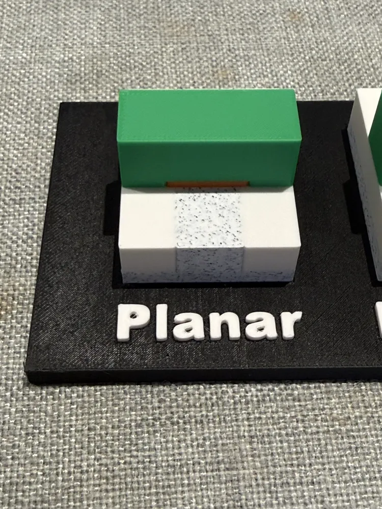
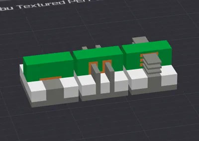
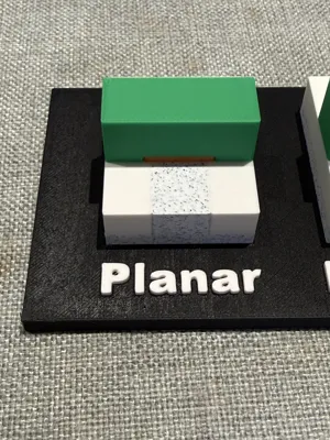
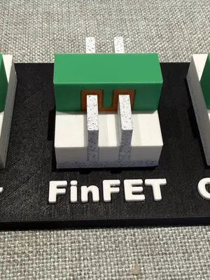
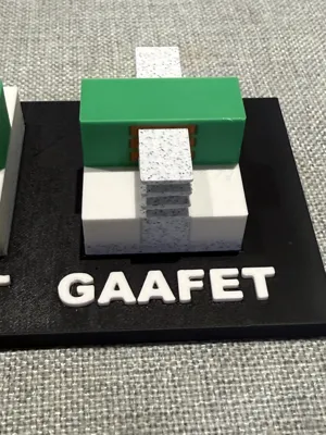
This model visually demonstrates the progression of transistor architectures from Planar → FinFET → GAAFET, making it perfect for:
- 📚 Teaching semiconductor fundamentals
- 🎓 Classroom demonstrations & lab displays
- 🧠 Engineering students & IC designers
- 🏠 Unique desk decoration for tech enthusiasts
Each structure is carefully designed to highlight the key geometric differences between transistor generations, making complex concepts intuitive and easy to understand.
✨ Features:
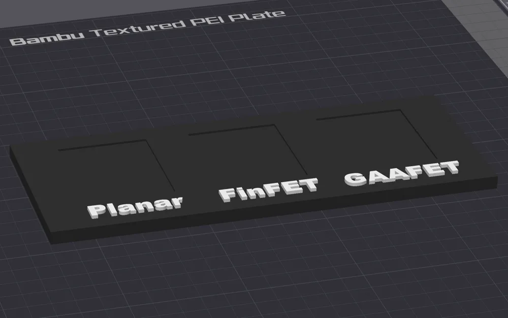
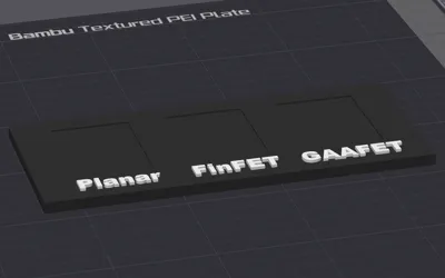
- Clean, modular design with labeled base
- Optimized for multi-color 3D printing (AMS friendly)
- No supports required (depending on slicer settings)
- Compact and professional-looking display piece
- Great conversation starter for your desk or lab
Whether you're an EE, student, or semiconductor nerd, this model turns cutting-edge chip technology into something you can hold in your hand.
License

You shall not share, sub-license, sell, rent, host, transfer, or distribute in any way the digital or 3D printed versions of this object, nor any other derivative work of this object in its digital or physical format (including - but not limited to - remixes of this object, and hosting on other digital platforms). The objects may not be used without permission in any way whatsoever in which you charge money, or collect fees.


Comment & Rating (2)