
Silicon wafer precision scribing system
Print Profile(1)

Description
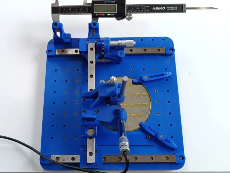
This design is a precision scribing system for silicon wafer. For a better idea of how its used please look at this video:
In microelectronic, multiple devices are made on silicon wafers by photolithography before the wafer is cut to separate each device. Dicing is generally done with special saws but it is also possible (and more economical) to use a diamond tip to scratch (scribe) the wafer and break (cleave) it over its crystalline directions. This device is designed to make the scribing more precise at a low cost. It can also be used for glass.
Here is a detailed building guide on Instructables.
To build this device you will need:
- Linear rail: 3X 20cm long MGN12 rails with 3X MGN12C (short) blocks and 1X MGN12H (long) block
- Linear rail: 1X 7.5cm MGN7 rail with 1X MGN7H (long) block
- Small digital pen microscope
- Micrometer head 1X 0-13mm and 1X 0-6.5mm
- Various M3 and M2 bolts and nuts
- M3 4.2mm diameter 4mm long melt inserts
If you like this model you may also have a use for my 3D printed cleaving pliers. They come quite handy when making small wafer fragments.
Boost Me (for free)
If you feel like it you can boost this model. If will help others to discover it and give me some credit to buy filament.
License

You shall not share, sub-license, sell, rent, host, transfer, or distribute in any way the digital or 3D printed versions of this object, nor any other derivative work of this object in its digital or physical format (including - but not limited to - remixes of this object, and hosting on other digital platforms). The objects may not be used without permission in any way whatsoever in which you charge money, or collect fees.


Comment & Rating (12)